Description
BJT Transistor Experimentation Board
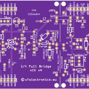
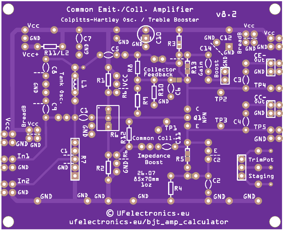
This board is designed for experimenting with NPN transistor–based amplifier and oscillator circuits without designing and manufacturing a dedicated PCB for every new circuit.
Whether you’re learning transistor fundamentals, developing a small analog circuit, or testing amplifier ideas before designing a final PCB, this board provides a flexible platform for rapid experimentation.
Suitable for:
- Students
- Hobbyists
- Makers
- Educational labs
- Analog electronics enthusiasts
New in Version 8.2
Compared to v8.1, version 8.2 adds additional footprints for:
- Breadboard-friendly input and output pin header footprints.
- Breadboard power connection footprints for both the input and output sides.
- Optional jumper locations south of C10 and between R4 and C2.
- A staging area for testing trimmers before permanent installation (using a female pin socket).
- Increased spacing in several areas for easier assembly and soldering.
Supported Circuit Types
- Common Emitter amplifiers
- Common Collector amplifiers
- Colpitts oscillators
- Hartley oscillators
- Treble boosters
- Multi-stage transistor amplifiers
- Signal buffering stages
- Small-signal analog experiments
…and many custom transistor circuits.
Link to the page with Circuit Library & Teaching Ideas
Key Features
Designed for Reuse
=> Instead of designing and manufacturing a new PCB for every amplifier idea, this board allows many analog transistor circuits to be assembled, modified and reused on the same platform.
Semi-Schematic PCB Layout
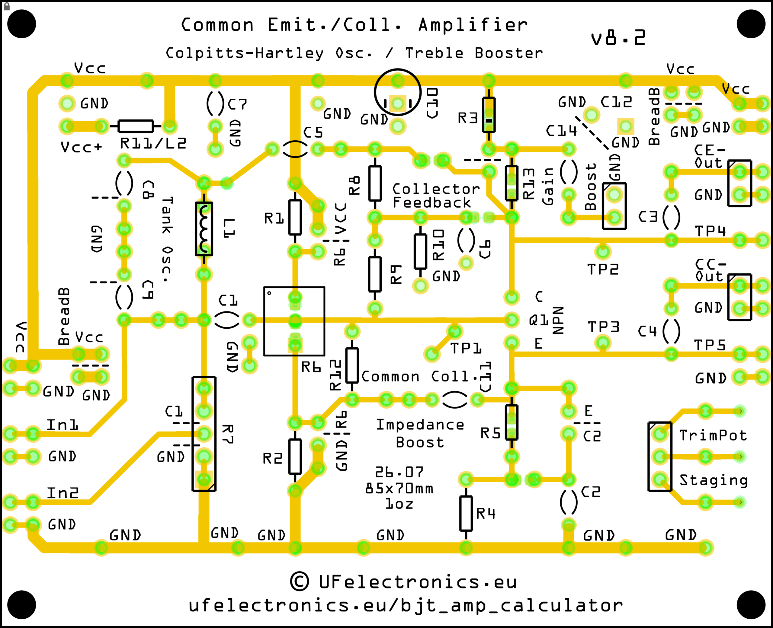
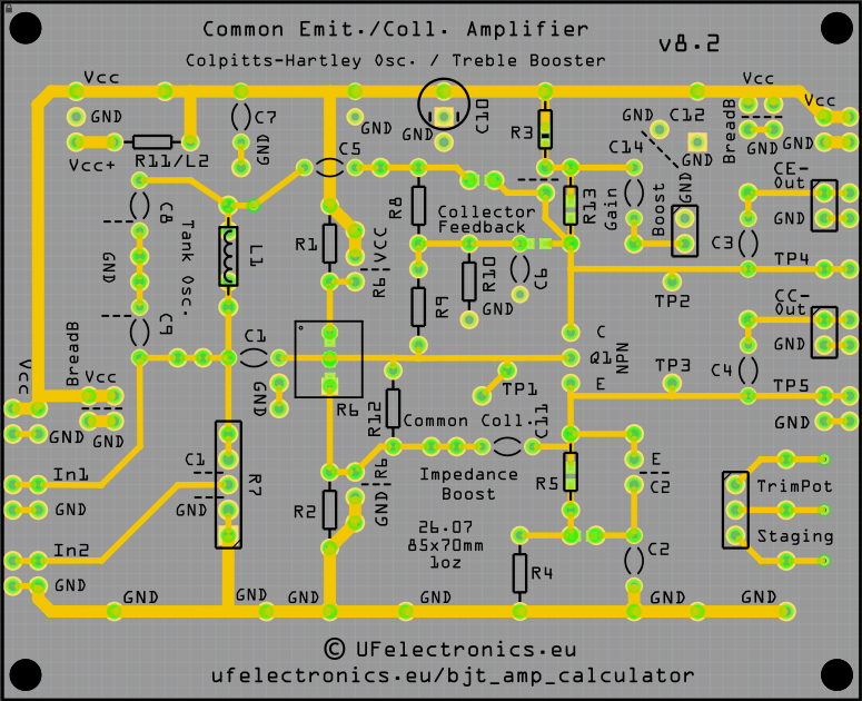
=> The board visually follows the signal flow of the circuit, helping users relate schematics to their physical implementation.
Visible Signal Routing
=> Signal traces are intentionally placed on the component side instead of underneath the board, making it easier to follow the circuit while probing and debugging. – The purple solder mask improves trace visibility, making the signal routing easier to follow during assembly, debugging and learning..
Through-Hole Design
=> Easy to solder, modify, debug, and reuse.
Full Backside Ground Plane
=> Improves grounding and reduces noise.
Configurable Footprints
=> Multiple optional footprints allow quick reconfiguration without cutting traces or redesigning the PCB.
Adjustable Biasing Support
=> Variable resistor footprints simplify transistor bias adjustment during experimentation.
Optional Supply Filtering
=> Add a resistor, ferrite bead or inductor together with nearby decoupling capacitors to investigate how supply filtering affects amplifier performance.
Integrated Test Points
=> Convenient probe points for measuring transistor base, collector and emitter voltages during circuit development.
Lab-Friendly Connectors
=> Power, signal and ground connections are arranged in adjacent pairs to simplify oscilloscope and laboratory measurements.
Collector Load Options
=> The collector resistor can optionally be divided into two stages for experiments with gain enhancement and frequency-dependent feedback.
Spacious Layout
=> Extra spacing between components improves probing, soldering, and debugging.
Educational Value
- Transistor biasing
- Voltage gain
- Emitter degeneration
- Phase inversion
- AC coupling
- Bypass capacitors
- Supply filtering
- Oscillator design
- Feedback techniques
- Impedance matching concepts
- Analog debugging techniques
Link to the page with Circuit Library & Teaching Ideas
Board Specifications
- PCB Size: 82 mm × 70 mm
- PCB Thickness: 1.6 mm
- Copper Weight: 1 oz
- Through-hole construction
- Full backside ground plane
PDF with Description
Click here for link to the PDF (Rev. 1)
Assembly Sheets
PDF – ODS (LibreOffice) – Excel (Microsoft)
Suggestions?
Why start with simple amplifiers?
A single-transistor amplifier may seem simple, and it is. But that simplicity is also its greatest strength as a learning tool.
When you build, tweak, and measure these circuits yourself, you quickly discover the gap between theoretical calculations and practical reality. Biasing is rarely perfect, gain is limited, and small changes can have large effects.
This hands-on experience builds the intuition that every analog designer needs.
As these limitations become clear, the motivation to move toward more advanced circuit topologies naturally arises. In that context, the differential amplifier stands out as a powerful next step, offering significantly improved stability, linearity, and control.
This board is therefore not just a tool for learning how transistor amplifiers work, but for understanding why more advanced designs are needed.
It is through these limitations that real understanding begins.