Description
Learn MOSFETs, BJTs, Gate Drivers and H-Bridges – One Output Stage at a Time
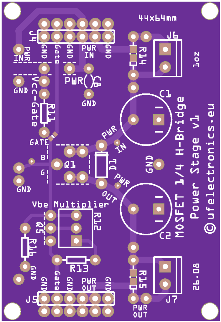
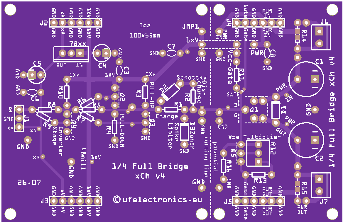
The 1/4 H-Bridge xCh v4 is an educational and experimentation PCB for learning how MOSFET and BJT power transistors really work.
Rather than presenting a finished motor driver or power amplifier, this board exposes the individual building blocks that make up real output stages. You decide how they are connected, experiment with different configurations, and observe the results using a multimeter or oscilloscope.
The PCB is equally suited for electronics hobbyists, engineering students, educators, and anyone wanting to understand power electronics beyond the application notes.
The design supports both MOSFETs and power BJTs, allowing you to explore everything from direct MCU gate drive to push-pull gate drivers, Class AB output stages and complete H-bridges.
What can you learn?
With a single board you can experiment with:
- Direct MCU drive (3.3 V / 5 V)
- Logic-level MOSFETs
- Gate resistor selection
- Gate charging and discharging
- Switching speed
- Switching losses
- Miller plateau
- Flyback diodes
- Gate voltage protection
- Pull-up and pull-down drivers
- Push-pull (totem-pole) gate drivers
- VBE multipliers
- Class A and Class B transistor stages
- MOSFET and BJT characterization
Connect two boards together and you can explore:
- Half H-bridges
- Push-pull output stages
- Class AB amplifier output stages
Connect four boards together and build a complete H-bridge.
Designed for Learning
Unlike production PCBs, this board has been designed specifically for experimentation.
Features include:
- Through-hole components throughout.
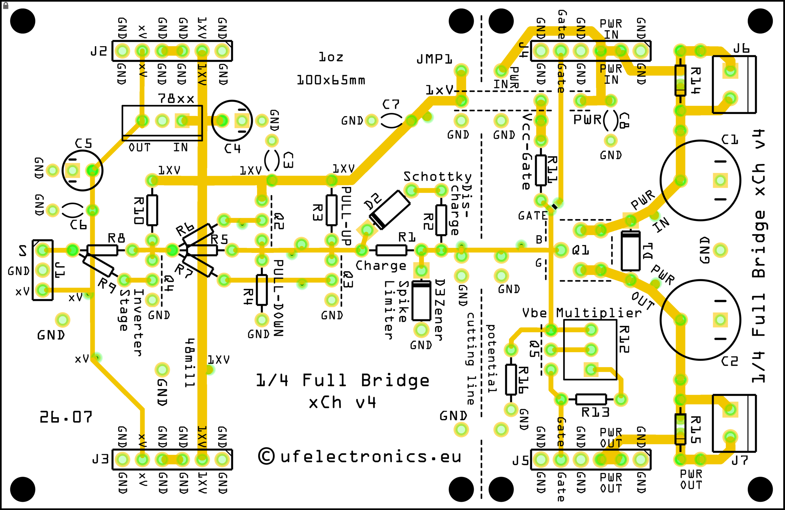
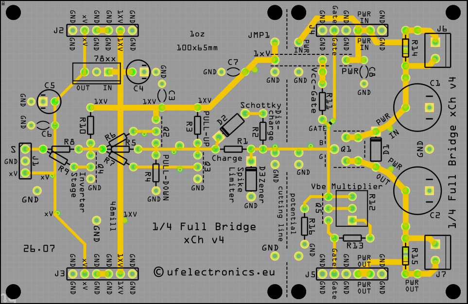
- Semi-schematic component placement.
- Visible top-layer routing.
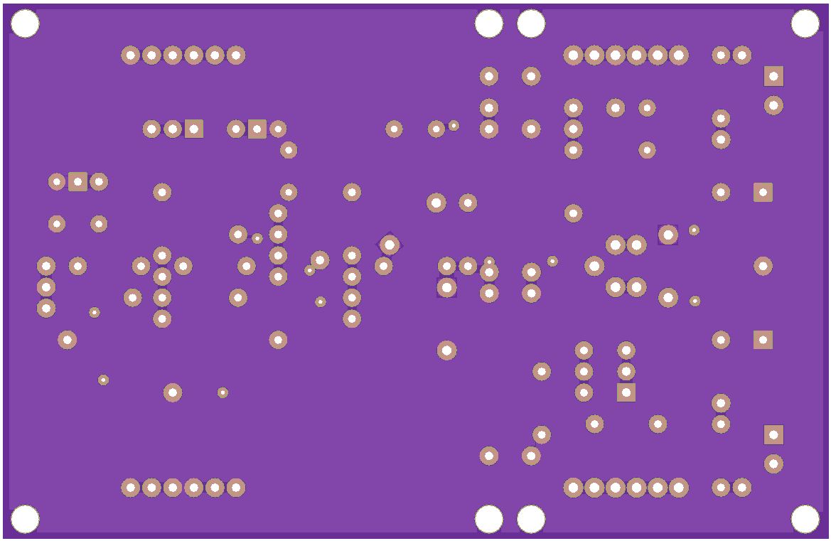
- Full ground plane on the opposite side.
- Numerous measurement points.
- Modular sections that can be populated individually.
The objective is to make the transition from circuit schematic to physical PCB as intuitive as possible while making measurements and modifications easy.
Flexible Signal Conditioning
The left side of the PCB contains optional signal-conditioning blocks that can be combined as needed.
Available functions include:
- Logic inversion
- Default OFF configuration
- Default ON configuration
- Push-pull gate driver
- High-voltage gate drive
- Independent gate charge and discharge control
- Gate spike protection using a Zener diode
Whether you simply want to drive a logic-level MOSFET directly from a microcontroller or build a higher-current gate driver, the required building blocks are already available on the PCB.
Output Stage Experiments
The right side of the PCB focuses on the output transistor itself.
Features include:
- External gate/base drive connector
- Direct access to drain/collector and source/emitter
- Optional series resistors
- Flyback diode footprint
- Integrated VBE multiplier for Class AB amplifiers
- Adjustable bias current
- Thermal compensation capability
This makes the board suitable for experimenting with both switching applications and linear amplifier output stages.
Modular by Design
One of the unique features of the board is its modular construction.
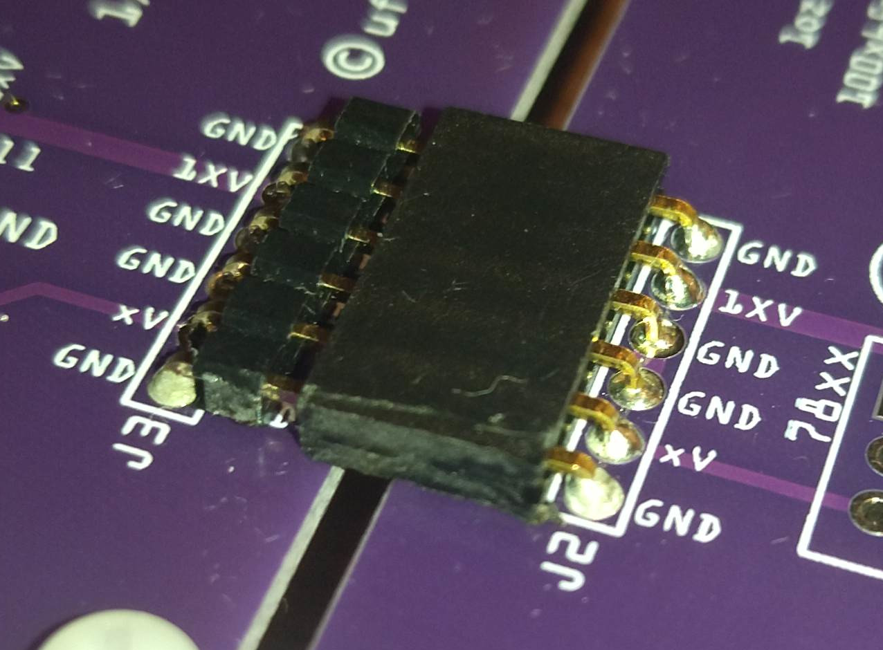
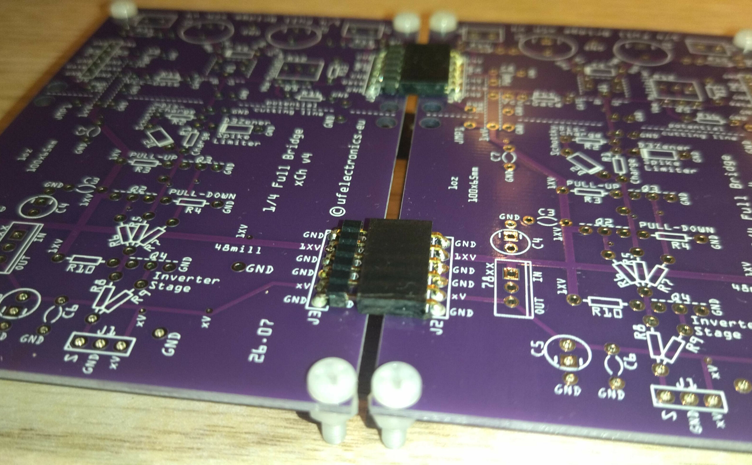
The PCB can optionally be divided into two smaller sections, allowing only the required circuitry to be used.
If required later, the two sections can simply be plugged together again using right-angle pin headers.
Likewise, multiple boards can easily be interconnected to build larger circuits ranging from a single transistor stage to a complete H-bridge.
Typical Applications
- Learning power electronics
- University laboratory exercises
- Electronics education
- Gate driver development
- MOSFET evaluation
- BJT evaluation
- Class AB amplifier experiments
- Motor driver experiments
- H-bridge development
- General transistor characterization
Who is this board for?
- Electronics hobbyists
- Engineering students
- Teachers and educators
- Makers
- Professional engineers wanting a flexible experimentation platform
Documentation Included
The board includes a comprehensive documentation package explaining both the PCB layout and the underlying electronics.
Topics include:
- Gate drive theory
- Push-pull drivers
- VBE multipliers
- Switching losses
- Gate transition control
- Flyback protection
- Decoupling
- Multi-board configurations
- Assembly examples
- SPICE simulations
Rather than simply showing where components go, the documentation explains why they are used and how different configurations affect circuit behaviour.
Download the documentation here ! (Rev. 1)
Set of two PCBs.
PCBs only – No components.