
Based on the Motorola Application Note AN-422
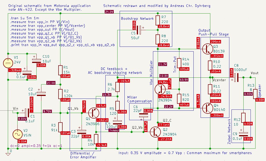
Many classic audio power amplifiers from the 1970s and 1980s were built around a small collection of elegant circuit techniques that remain relevant today. One such example is the Motorola AN-422 Class-AB amplifier topology.
While schematics of these amplifiers are widely available, understanding why each section exists is often more difficult than following the circuit itself. To address this, I prepared a document that walks through the amplifier one functional block at a time and explains the underlying design concepts rather than focusing purely on calculations and transistor-level details.
Download the Document
The Class-AB Amplifier Explained on a Conceptual Level
PDF:
KiCad Project Files
For readers who would like to study the circuit in greater detail, the KiCad project files are available on GitHub.
These files include the schematic and provide a practical starting point for simulation, PCB development, component modifications, and further experimentation with the Motorola AN-422 inspired design.
GitHub Repository:
https://github.com/ufelectronics/classab-based-on-motorola-an-422
Contributions, suggestions, and improvements are welcome.
What Is Covered?
The document breaks the amplifier into its major building blocks and explains the purpose of each section:
- Input coupling and bias networks
- The input error amplifier
- The feedback network
- Dominant-pole and compensation techniques
- Voltage Amplifier Stage (VAS)
- Bootstrap circuits
- VBE multiplier biasing
- Class-AB push-pull output stages
- Emitter resistors and local feedback
- Global negative feedback
- Zobel output networks
- Supply decoupling and stability considerations
Rather than treating the amplifier as one large schematic, every functional block is examined individually and then placed back into the larger signal flow.
Why This Amplifier Topology Is Interesting
The Motorola design demonstrates how a relatively small number of components can achieve good gain, low distortion, thermal stability, and reliable operation. Concepts such as bootstrapping, global negative feedback, emitter degeneration, and VBE multiplier bias control are all implemented in a straightforward and educational manner.
Although modern integrated amplifier solutions are common today, understanding these discrete transistor designs provides valuable insight into the foundations of analog electronics and audio amplifier architecture. The same design principles can still be found inside many contemporary amplifier circuits.
Intended Audience
This document may be useful for:
- Electronics hobbyists
- Students learning analog circuit design
- Audio amplifier enthusiasts
- Engineers interested in classic transistor amplifier topologies
- Anyone wanting to understand how feedback-based power amplifiers work
The explanations are intentionally focused on concepts and architecture, making the material accessible even if you are not an experienced analog designer.
Notes
The schematic discussed in the document is based on Motorola Application Note AN-422 and has currently only been simulated. No physical prototype or laboratory measurements have been performed yet.
Special thanks are given in the document to Clyde S. for sharing the original schematic and to Eric Habets for providing additional technical explanations and insights.