Investigating how basic components work is my guiding principle in this part of the DIY buck converter project, too.
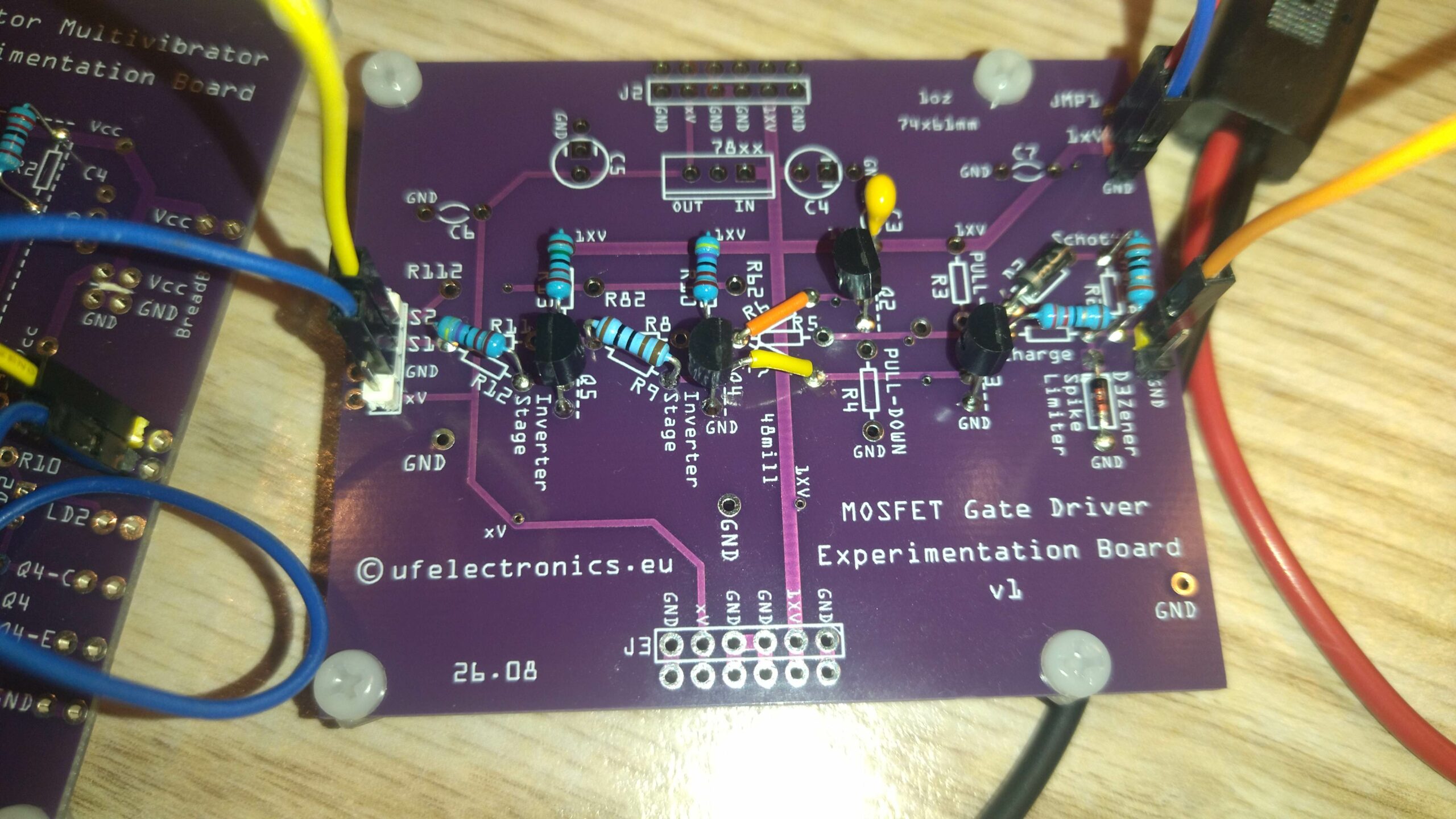
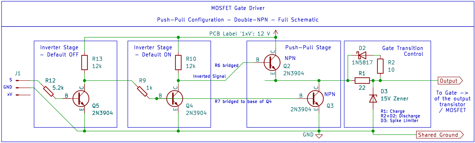
The circuit is built around a push-pull output stage, with several refinements and some essential supporting components.
* Q2 and Q3 – Push-pull stage: Q2 sources current to charge the MOSFET gate; Q3 sinks current to discharge it.
* Q4 and Q5 – Input stages: Two common-emitter stages condition the input signal and control the push-pull stage.
* R1 and R2 – Gate resistors: Set the resistance in the gate’s charging and discharging paths.
* D2 – Schottky diode: Provides a separate discharge path, allowing faster turn-off while retaining a separate higher charging resistance to help damp potential oscillations.
* D3 – Zener diode: Protects the MOSFET against excessive gate-source voltage, including voltage spikes.
Why use a transistor push-pull stage instead of driving the MOSFET directly with a 5 V signal?…
… A higher gate-drive voltage allows the MOSFET to switch faster, reducing the time it spends in the transition between on and off states. => Shorter transitions can reduce switching losses in the MOSFET.
The gate driver…
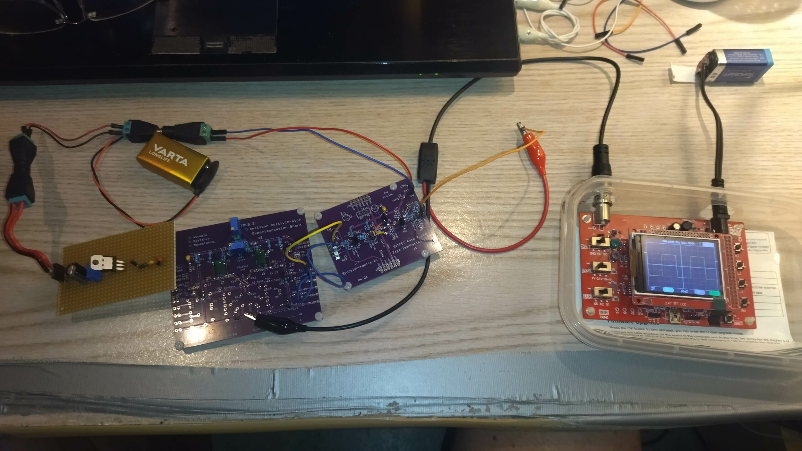
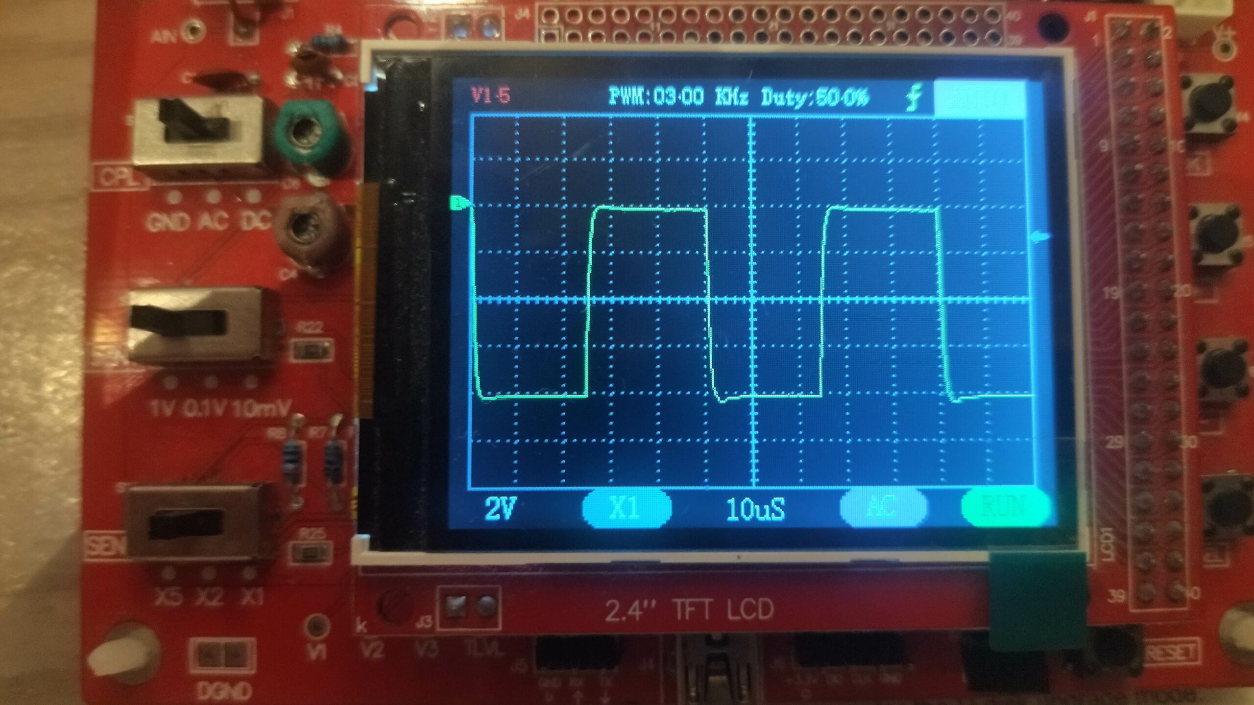
* receives its switching signal from an astable multivibrator
* drives the MOSFET in the buck converter – the next small project.
This circuit will be tested with a MOSFET in the buck converter over the next few days.
The pre-coupled astable multivibrator can be found here: No signal generator? – Build a variable astable multivibrator